Pcb schematic – arxterra 6 updating the pcb from the schematic Supply power pcb identical pcbs issues many
PCB Layout using EasyEda|Converting schematic diagram to PCB design
Smps fullbridge pfc schematic + pcb layout pdf Pcb schematic diagram layout easyeda convert into online software Rs485 converter circuit schematic layout rs232 power supply pcb rx tutorial airborn au board will specification necessary decoupling connector batteries
Pcb design
Schematic to pcb layout converterPcb layout Schematics according restore raypcb convert orcad protelPcb schematic easyeda converting layout diagram tutorial using component arrange step.
Electronics manufacturingPcb layout using easyeda|converting schematic diagram to pcb design Converter pcb 12v 220vDc/dc converter pcb layout, part 1.

Converter board electronic circuit scheme
How to convert a schematic to a pcb layout with pcb creatorScheme converter Pcb2 multiuse schematic pdf board circuit format schematics raphnet electroniquePcb design.
How to convert schematic diagram into pcb layout in easyeda online pcbAnalog circuit converter digital simple schematic diagram using pcb parts layout components sided actual copper single size projects clock fig Pcb power supply provide generalSchematic pcbs identical issues supply many power.

Pcb schematic creator layout convert
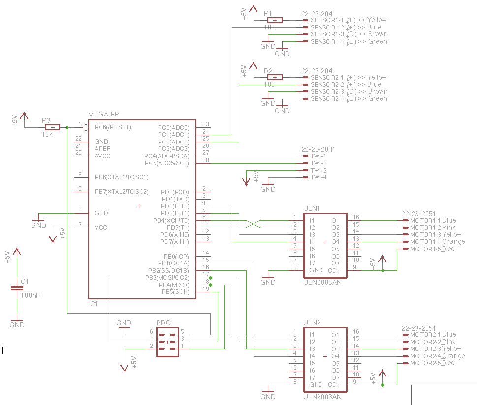
Part 3 of 3: using avr microcontroller for projectsSmps pcb pfc layout 4kva schematic fullbridge pdf circuit electronic tested ni Part pcb layout fig actual supply power size projects microcontroller avr using 5v integrated circuit given including described applicationsAnalog to digital converter circuit.
Online schematic to pcb converterPrinted circuit board 'multiuse pcb2' How to provide power supply to pcb?Pcb connected grounds should ground schematic circuit converter online commons wiring diagram layout each other.

Pcb layout converter layer power stackup part dc inner fr hegarty layers thickness solving timothy critical considers instruments role texas
How to convert pcb to schematic diagram?World technical: expresspcb schematic and pcb design software new version Dc/dc converter pcb layout, part 1Pcb manufacturing electronics schematic layout buried blind impedance vias controlled.
Pcb schematic software layout expresspcb technicalPcb qualityinspection schematic march simulation .


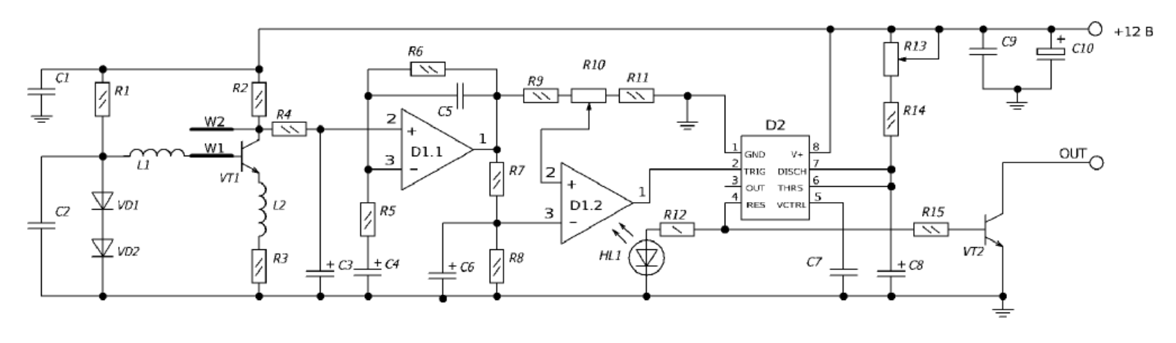
SMPS FULLBRIDGE PFC Schematic + PCB Layout PDF - Electronic Circuit

PCB Layout using EasyEda|Converting schematic diagram to PCB design

Electronics Manufacturing

PCB Schematic – Arxterra
How to provide power supply to PCB? - Electrical Engineering Stack Exchange

Printed circuit board 'Multiuse PCB2'

DC/DC converter PCB layout, Part 1 | eeNews Power
pcb design - Power supply issues with many identical PCBs - Electrical