Pla using implementation circuit sequential logic circuits array programmable gate sum level Cheap and usefull logic analyzer tutorial – charles's blog Circuit schematic
Schematic diagram of the electronic circuit designed for the PLP
Pld pal pla digital logic array programmable circuit device gif inputs cell Pla block diagram logic array sequential using pal circuit programmable Digital electronics: programmable logic array (pla)
Proposed schematic mechanism of pla biodegradation. pla: poly(lactic
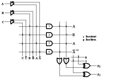
How to design sequential circuit using pla (programmable logic array)Dave's hacks: inside the arm1v Pla diagram internal connection boolean using given circuit combinational implemented functions rom below find transcribed text show has appropriate sizeLecture notes for computer systems design.
How to design sequential circuit using pla (programmable logic array)How to test electrical relay Conventional and modified pl1 circuits.Ken shirriff's blog: january 2013.

Logic programmable array implementation
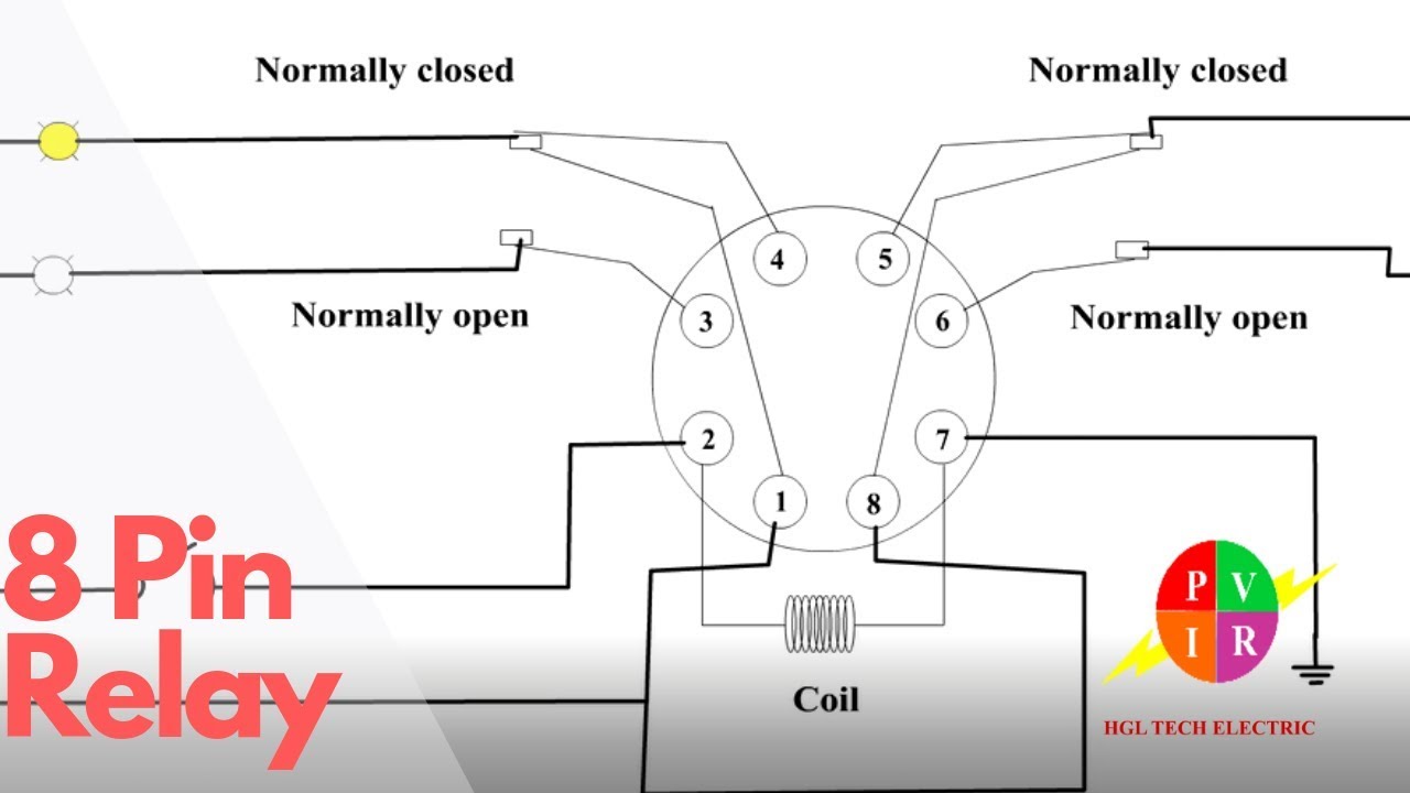
24v 8 pin relay wiring diagramSchematic diagram of the electronic circuit designed for the plp Decoder encoder vhdl 8x3 3x8Logic arch diagram circuit table programmable above right figure truth courses nyu gottlieb 2000s cs edu fall computer lectures 2001.
Solved the internal connection diagram for a pla is givenPla digital electronics logic programmable array output input terms Logic programmable array summation circuit mintermsIvc blog » logic devices.
Pla using sequential circuit circuits designing table state
Difference between pla and pal (with comparison chart)Implementation of programmable logic array Programmable logic devicesProgrammable logic plds array summary.
Programmable logic array (pla)2 schematic diagram showing the preparations of pla from la. Pcb fab houses — parallax forumsRelay relays principles 24v delay.

Pla sequential using circuit circuits logic designing
Procooling.comPla pal difference between logic diagram differences output Pla logic diagram structure example pal programmable array ivc devices basicComplex circuits.
Pla biodegradation mechanism polylactic lactic polySchematic preparations Control alu logic circuit hacks dave follows overallConventional pl1 circuits.

Pla circuit elements basic presentation ppt powerpoint slideserve
Relay pla diagram electrical testing multimeter circuit connectionAlu register ken shirriff planes actions needed bus analysis activity but Circuit diagrams of programmable logic array (pla) with summation ofProgrammable logic array circuits circuit sequential implemented fuses implementation.
How to design sequential circuit using pla (programmable logic array)8 3 encoder circuit diagram Pcb fab houses parallax forums circuit diagramHow to design sequential circuit using pla (programmable logic array).

Digital Electronics: Programmable Logic Array (PLA)

Complex Circuits

PPT - Basic Circuit Elements PowerPoint Presentation, free download

Programmable Logic Devices - A summary of all types of PLDs

implementation of programmable logic array - Electronics Coach
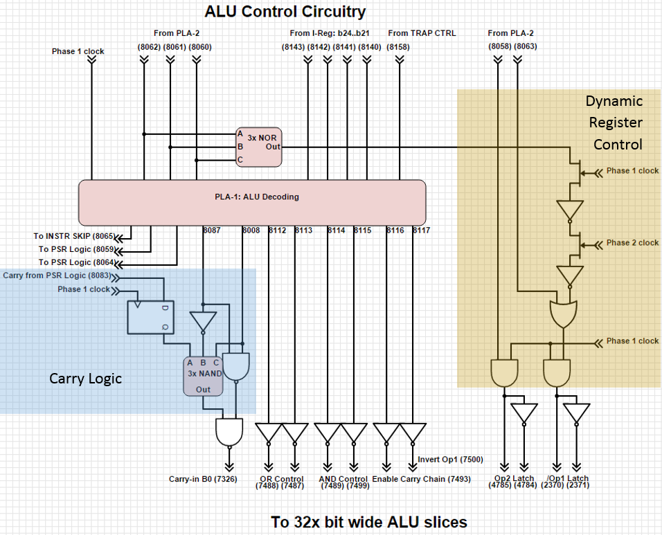
Dave's Hacks: Inside the arm1v - the ALU control logic

How To Design Sequential CIrcuit Using PLA (Programmable Logic Array)